


Customer Case Analysis Report
Project Background
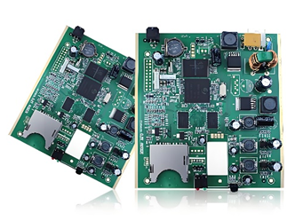
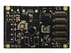
As electronics technology advances, printed circuit boards (PCBs) are becoming increasingly vital in various electronic devices. The quality of PCB photoresist is crucial to the performance and reliability of circuit boards. Our company provides several resin materials for PCB photoresist, which have been successfully and consistently applied in mass production by domestic PCB photoresist companies. These materials are used in products such as automotive PCT-resistant inks and black matte solder masks. Our company is a key core material supplier to these enterprises.
Customer Needs and Challenges
High-performance PCB photoresist materials must meet the following stringent requirements:
High Temperature Resistance: Capable of withstanding high-temperature environments, particularly common in automotive electronics.
Excellent Adhesion: Ensuring firm attachment to the PCB, preventing detachment during use.
Outstanding Chemical Resistance: Able to withstand various chemicals such as acids, bases, and solvents.
Good Electrical Insulation: Ensuring insulation between electronic components to prevent short circuits.
Environmental Requirements: Complying with RoHS and REACH environmental regulations to ensure green and eco-friendly materials.
Our Solution
To address the needs and challenges of our customers, we developed several resin materials specifically designed for PCB photoresist, featuring:
High Temperature Resistance Formula: Utilizing innovative chemical formulations to enhance the high-temperature resistance of resin materials, suitable for automotive applications.
Enhanced Adhesion: Advanced material technology to improve resin adhesion to the PCB, ensuring long-term stability.
Excellent Chemical Resistance: Resin materials exhibit outstanding resistance to acids, bases, and solvents, ensuring chemical stability.
High Electrical Insulation: The materials provide excellent electrical insulation, ensuring the electrical safety of the PCB.
Green and Eco-friendly: Strict control over raw materials and production processes to ensure products meet international environmental regulations.
Application Examples
Automotive PCT-resistant Ink:
High Temperature Resistance: Our resin materials perform excellently in high-temperature environments, ensuring the stability and reliability of automotive PCBs under extreme temperature conditions.
Durability: Multiple tests have proven that resin materials in automotive PCT-resistant inks can maintain excellent performance over time, including high-temperature, humidity, and corrosion resistance.
PCB Black Matte Solder Mask:
Outstanding Appearance and Performance: Our resin materials enable PCB black matte solder masks to have excellent visual effects while maintaining superior mechanical performance and chemical stability.
Environmental Performance: The product complies with RoHS and REACH standards, meeting environmental requirements and ensuring global market compliance.
Customer Feedback
Through close collaboration and extensive testing with our customers, our resin materials have performed excellently in actual applications, receiving high praise:
Domestic Leading PCB Companies: Customers stated that our resin materials in automotive PCT-resistant inks and PCB black matte solder masks significantly exceeded performance expectations, demonstrating stability and meeting the stringent requirements of high-end electronic products.
Ongoing Collaboration: Customers expressed satisfaction with our stable supply and quality assurance of materials and look forward to continued cooperation in future projects.
Success Factors
Technical Advantage: Our technical advantages in PCB photoresist resin material development ensure that products excel in temperature resistance, adhesion, chemical resistance, and electrical insulation.
Customer Orientation: Through close collaboration with customers and fully understanding and meeting their needs, we provide customized solutions.
Quality Control: A strict quality control system ensures product consistency and reliability, meeting the rigorous requirements of high-end electronic products.
Environmental Awareness: Adhering to a green and eco-friendly philosophy ensures our products comply with international environmental regulations, offering sustainable material choices to our customers.
Future Outlook
The success of this project not only demonstrates our company's R&D and production capabilities but also showcases our competitive advantage in the high-performance PCB photoresist market. In the future, we will continue to commit to innovation and quality improvement, providing better materials and services to our customers and promoting the development of the electronics industry.
This case analysis report details our successful experience in applying PCB photoresist resin materials to high-end electronic products, showcasing our product's technical advantages and market recognition. We hope it will positively contribute to the company's brand image and market expansion.

