


Photoresist, also known as photoresist, is a mixed liquid that is sensitive to light. Its components include: photoinitiator (including photosensitizer, photoacid generator), photoresist resin, monomer, solvent and other additives. Photoresist can transfer the required fine pattern from the mask (mask) to the substrate to be processed through photochemical reaction, exposure, development and other photolithography processes. Depending on the usage scenario, the substrate to be processed here can be an integrated circuit material, a display panel material or a printed circuit board. 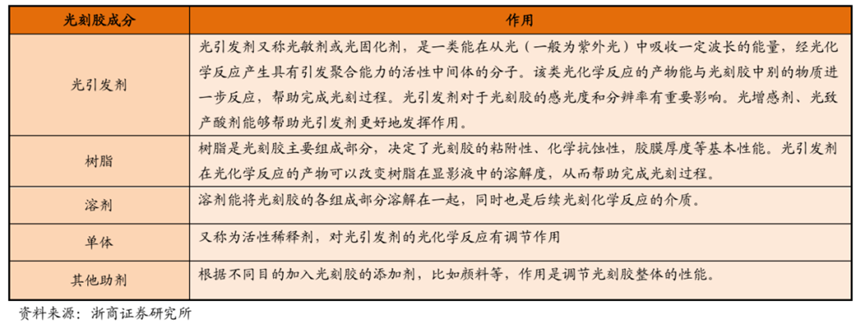
According to statistics from Zhiyan Consulting, a third-party organization, the global photoresist market size is expected to be nearly US$9 billion in 2019, with a CAGR of approximately 5.4% from 2010 to September 2020. It is expected that the global photoresist market size will exceed US$10 billion by 2022. Photoresists can be classified into PCB photoresists, display panel photoresists, semiconductor photoresists and other photoresists according to their application areas. The market structure of different types of photoresists in the global market is relatively balanced, and the specific proportion can be shown in the figure below. 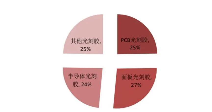
Global photoresist market structure Data from Zhiyan Consulting also shows that benefiting from the trend of the semiconductor, display panel, and PCB industries moving eastward, the annual growth rate of China's local photoresist supply reached 11% from 2011 to 2020, higher than the global average growth rate of 5%. At present, China's local photoresist is mainly used for PCB, and the supply of photoresist for flat panel displays and semiconductors accounts for a very low proportion. The production structure of China's local photoresist companies can be shown in the figure. 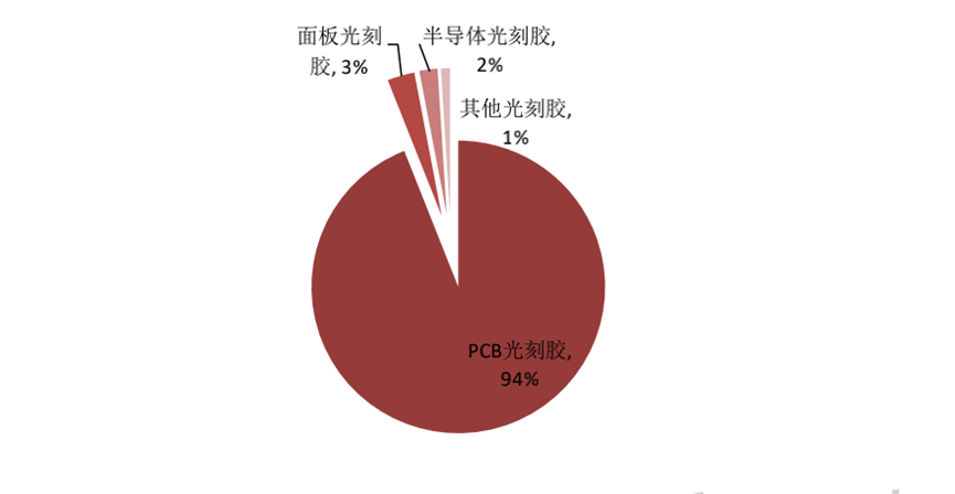
Production structure of China's local photoresist companies
Photoresist classification In the flat panel display industry , the main photoresists used are color and black photoresists, photoresists for LCD touch screens, TFT-LCD positive photoresists, etc. In the photolithography and etching production process, photoresists are coated on the surface of the crystal film, and the pattern on the mask (mask) is transferred to the film through exposure, development and etching processes to form a geometric pattern corresponding to the mask.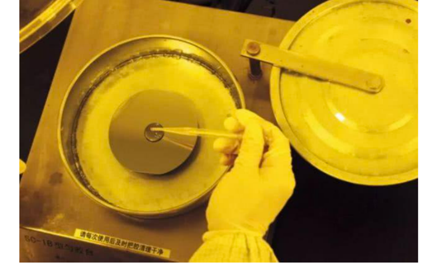
In the PCB industry , the main photoresists used are dry film photoresist, wet film photoresist, photosensitive solder resist ink, etc. Dry film is a special film attached to the treated copper-clad board for exposure and development; wet film and photo-imaging solder resist ink are coated on the copper-clad board and exposed and developed after drying. Dry film and wet film each have their own advantages. Generally speaking, wet film photoresist has higher resolution than dry film and lower price, and is replacing some markets of dry film photoresist. 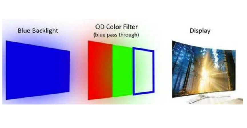
The manufacture of color filter film for LCD screen depends on color photoresist . In the semiconductor integrated circuit manufacturing industry , g-line photoresist, i-line photoresist, KrF photoresist, ArF photoresist, etc. are mainly used. In the manufacturing process of large-scale integrated circuits, silicon wafers are generally subjected to more than ten times of photolithography. In each photolithography and etching process, the photoresist must go through pre-baking, coating, pre-baking, alignment, exposure, post-baking, development and etching to transfer the pattern on the mask (mask) to the silicon wafer. 
Photosensitive solder mask ink is used for PCB Photoresist is an important material for integrated circuit manufacturing. The quality and performance of photoresist are key factors affecting the performance, yield and reliability of integrated circuits. The cost of the photolithography process is about 35% of the entire chip manufacturing process, and the time consumed accounts for about 40%-50% of the entire chip process. Photoresist materials account for about 4% of the total cost of IC manufacturing materials, and the market is huge. Therefore, photoresist is the core material for semiconductor integrated circuit manufacturing. 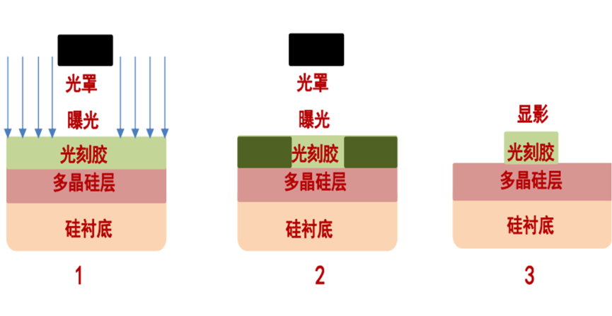
Schematic diagram of positive photoresist development According to the display effect , photoresists can be divided into positive photoresists and negative photoresists. The pattern formed by negative photoresist during development is opposite to the mask (mask); the pattern formed by positive photoresist is the same as the mask. The production process of the two is basically the same, and the difference lies in the main raw materials. 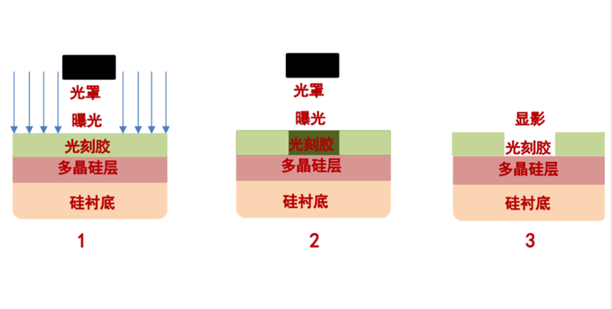
Schematic diagram of negative photoresist development According to the chemical structure , photoresists can be divided into photopolymerization type, photodecomposition type, photocrosslinking type and chemical amplification type. Photopolymerization type photoresists use olefin monomers to generate free radicals under the action of light, further initiate monomer polymerization, and finally generate polymers. 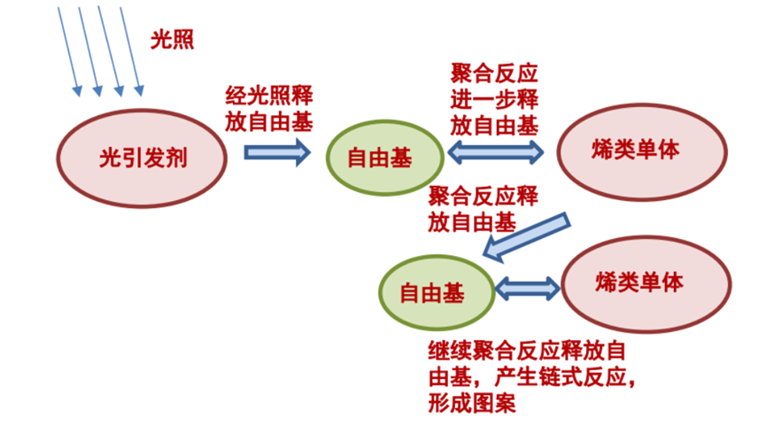
Schematic diagram of photopolymerization reaction. Photodecomposable photoresist uses materials containing diazoquinone compounds (DQN) as photosensitizers. After exposure to light, photodecomposition reaction occurs and can be made into positive photoresist. Photocross-linking photoresist uses polyvinyl laurate and other photosensitive materials. Under the action of light, it forms an insoluble network structure, which plays an anti-corrosion role and can be made into negative photoresist.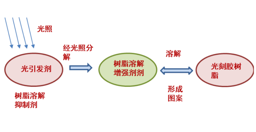
Schematic diagram of photodecomposition reaction After semiconductor integrated circuit lithography technology began to use deep ultraviolet (DUV) light source, chemical amplification (CAR) technology gradually became the mainstream of industry applications. In chemical amplification photoresist technology, the resin is polyethylene that is protected by chemical groups and is therefore difficult to dissolve. Chemical amplification photoresist uses photoacid generator (PAG) as a photoinitiator. 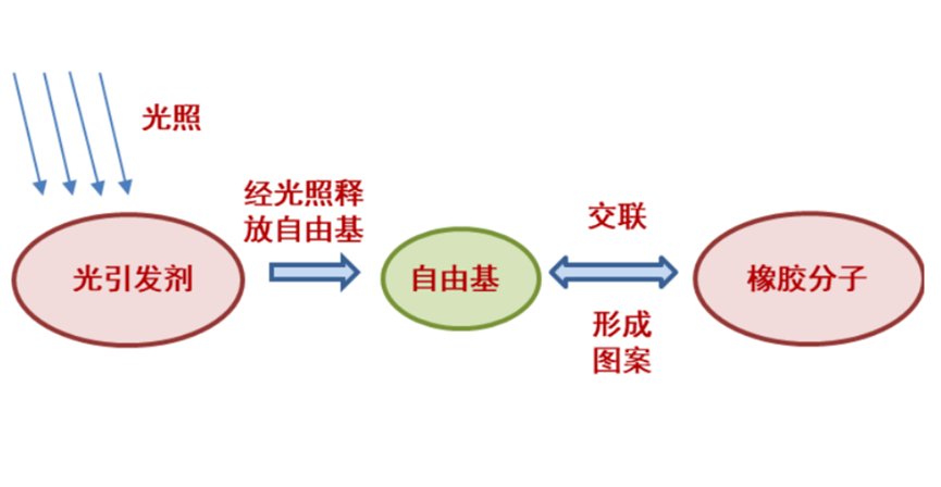
Schematic diagram of photocrosslinking reaction When the photoresist is exposed, the photoacid generator (PAG) in the exposed area will produce an acid. This acid acts as a catalyst during the post-heat baking process to remove the protective group of the resin, making the resin easy to dissolve. The exposure speed of chemical amplification photoresist is 10 times that of DQN photoresist, and it has good optical sensitivity to deep ultraviolet light source, and has the advantages of high contrast and high resolution. 
Schematic diagram of chemical amplification light reaction According to the exposure wavelength, photoresist can be divided into ultraviolet photoresist (300~450nm), deep ultraviolet photoresist (160~280nm), extreme ultraviolet photoresist (EUV, 13.5nm), electron beam photoresist, ion beam photoresist, X-ray photoresist, etc. Photoresists with different exposure wavelengths are applicable to different photolithography limit resolutions. Generally speaking, when the same process method is used, the shorter the wavelength, the better the processing resolution.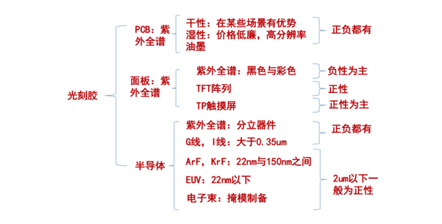
Summary of Photoresist Classification Photoresist is the "fuel" for the advancement of semiconductor process technology. In the field of integrated circuit manufacturing, if the photolithography machine is the "engine" that promotes the advancement of process technology, photoresist is the "fuel" of this "engine". The figure below shows how photoresist works in the manufacturing process of an NMOS transistor. NMOS transistors are one of the most commonly used integrated circuit structures in semiconductor process technology. 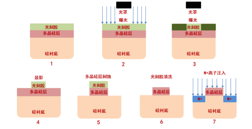
A manufacturing process of an NMOS transistor integrated circuit structure In such a typical example, the green part in step 1 represents the red part of the polysilicon material coated with a layer of photoresist. In the photolithography exposure process of step 2, the photoresist outside the black mask shielding range is irradiated by the photolithography light source, and the chemical properties are changed, which is manifested as a dark green in step 3. In step 4, after development, only the photoresist material is left above the polysilicon material represented by red where it was previously shielded by the mask. As a result, the pattern on the mask (mask) is transferred to the polysilicon material, completing the "photolithography" process. In the subsequent steps 5 to 7, based on the photoresist pattern left on the polysilicon material by the "photolithography" process, the "polysilicon layer etching", "photoresist cleaning" and "N+ ion implantation" processes jointly complete the construction of an NMOS transistor. The photoresist coating process in step 1 of the above figure is also an important semiconductor process. Its purpose is to establish a thin, uniform and defect-free photoresist film on the surface of the wafer. Generally speaking, the thickness of the photoresist film ranges from 0.5um to 1.5um, and the thickness error needs to be within plus or minus 0.01um. The main method of coating semiconductor photoresist is the spin coating method, which can be specifically divided into static spin method and dynamic spray method.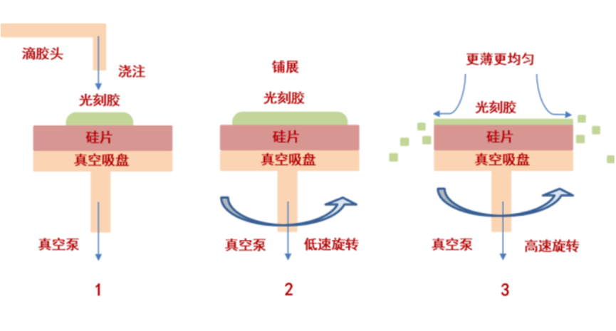
Schematic diagram of the static spin coating process Static spin method: First, the photoresist is deposited in the center of the silicon wafer through the glue dispensing head, then the photoresist is spread by low-speed rotation, and then the excess photoresist is shaken off by high-speed rotation. During the high-speed rotation process, part of the solvent in the photoresist will evaporate. This process can be shown in the figure below. 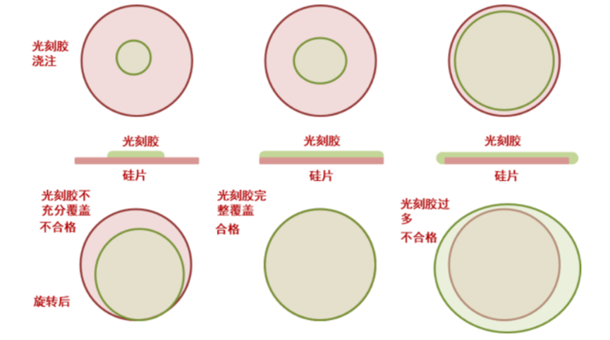
Schematic diagram of qualified and unqualified static coating process The amount of photoresist accumulation in the static coating method is very critical. If the amount is too small, the photoresist will not be able to fully cover the silicon wafer. If the amount is too large, the photoresist will accumulate at the edge of the silicon wafer or even flow to the back of the silicon wafer, affecting the process quality. Dynamic spraying method: As the size of silicon wafers becomes larger and larger, static coating can no longer meet the latest silicon wafer processing requirements. Compared with the static spinning method, the dynamic spraying method starts to rotate at a low speed at the moment when the photoresist is poured on the silicon wafer to help the photoresist to diffuse initially.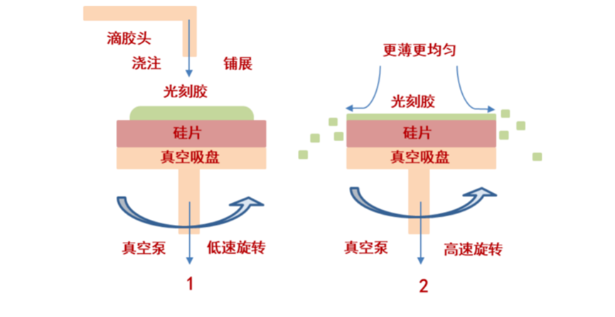
Schematic diagram of the dynamic spraying coating process. This method can use a smaller amount of photoresist to form a more uniform photoresist spread, and finally form a photoresist film that meets the thickness and uniformity requirements by high-speed rotation.
With the improvement of IC integration, the process technology level of integrated circuits in the world has entered the nanometer stage from the micron level, submicron level, deep submicron level. The trend of continuous reduction of integrated circuit line width has brought new challenges to semiconductor process technology including lithography. In the lithography process of semiconductor process, the characteristic size of integrated circuit line width can be determined by the Rayleigh formula as shown on the right: CD= k1*λ/NA 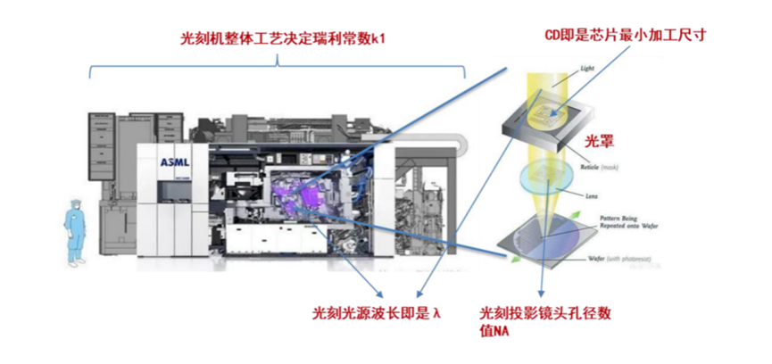
The meaning of each parameter in the Rayleigh formula CD (Critical Dimension) represents the characteristic size in the integrated circuit process; k1 is the Rayleigh constant, which is a correlation coefficient between process and material in the lithography system; λ is the exposure wavelength, and NA (Numerical Aperture) represents the aperture value of the lithography machine. Therefore, the lithography machine needs to reduce the Rayleigh constant and exposure wavelength and increase the aperture size to manufacture integrated circuits with smaller characteristic sizes. Among them, reducing the exposure wavelength is highly related to the light source and photoresist material used by the lithography machine. Historically, the wavelength of the light source used by the lithography machine has shown a trend of shrinking synchronously with the critical size of the integrated circuit. Lithography light sources of different wavelengths require completely different lithography equipment and photoresist materials. In the 1980s, the mainstream process size of semiconductor manufacturing was between 1.2um (1200nm) and 0.8um (800nm). At that time, lithography light sources with a wavelength of 436nm were widely used. In the first half of the 1990s, as the process size of semiconductor manufacturing evolved towards 0.5um (500nm) and 0.35um (350nm), lithography began to use 365nm wavelength light sources. The 436nm and 365nm light sources are the two spectral lines with the highest energy and the shortest wavelength in high-pressure mercury lamps. High-pressure mercury lamp technology is mature, so it was first used as a lithography light source. Using a short-wavelength, high-energy light source for lithography is easier to stimulate photochemical reactions and improve lithography resolution. Joseph Fraunhofer, a modern German scientist famous for his research on spectra, named these two wavelength spectra G-line and I-line respectively. This is also the origin of the names of g-line lithography and i-line lithography. Both g-line and i-line photoresists use linear phenolic components as the main resin and diazonaphthoquinone components (DQN system) as photosensitizers. The unexposed DQN components act as inhibitors, which can reduce the dissolution rate of photoresist in the developer by ten times or more. After exposure, the diazonaphthoquinone (DQN) group is converted into enone, and when in contact with water, it is further converted into indole hydroxy acid, which can be removed when the exposed area is developed with dilute alkaline water. As a result, the exposed photoresist will dissolve in the developer and be removed, while the unexposed photoresist portion will be retained. Although the components used in g-line photoresists and i-line photoresists are similar, their resins and photosensitizers have changes in microstructure, resulting in different resolutions. G-line photoresist is suitable for integrated circuits with a size of 0.5um (500nm) or more, while i-line photoresist is used for integrated circuits with a size of 0.35um (350nm) to 0.5um (500nm). In addition, both photoresists can be used in the production of larger electronic products such as LCD flat panel displays.
In the second half of the 1990s, following the guidance of Moore's Law, the size of semiconductor process technology began to shrink to below 0.35um (350nm) , thus requiring higher-resolution lithography technology. Deep ultraviolet light can be used as a lithography light source with higher resolution because of its shorter wavelength and smaller diffraction effect. With the development of research on rare gas halide excimer excited state laser light sources such as KrF and ArF, 248nm (KrF) and 193nnm (ArF) lithography light source technologies have matured and been put into practical use. However, due to the strong absorption effect of DQN system photoresist on the deep ultraviolet light band, the light generated by KrF and ArF as lithography gases cannot penetrate DQN photoresist, which means that the lithography resolution will be seriously affected. Therefore, deep ultraviolet photoresist adopts a completely different technical system from i-line and g-line photoresists. This technical system is called Chemically Amplified Resist (CAR). In the CAR technology system, the photoinitiator in the photoresist does not directly change the solubility of the photoresist in the developer after exposure, but produces acid. In the high temperature environment of the subsequent thermal baking process, the acid produced by exposure acts as a catalyst to change the solubility of the photoresist in the developer. Therefore, the photoinitiator under the CAR technology system is also called a photoacid agent. Since the acid produced by the photoacid agent of the CAR photoresist itself is not consumed during the exposure process but only exists as a catalyst, a small amount of acid can continue to play an effective role. CAR photoresist is highly photosensitivity and needs to absorb very little energy from deep ultraviolet radiation, which greatly enhances the efficiency of photolithography. The exposure speed of CAR photoresist is about 10 times that of DQN photoresist.
Since the second half of the 1990s, lithography light sources have begun to use 248nm KrF lasers; and since the 2000s, lithography has further turned to using 193nm wavelength ArF excimer lasers as light sources. Since then, for about 20 years until today, the 193nm wavelength ArF excimer laser has been the most reliable and widely used lithography light source in the field of semiconductor processes. Generally speaking, KrF (248nm) photoresists use poly(p-hydroxystyrene) and its derivatives as film-forming resins, and sulfonium iodonium salts and sulfonium salts as photoacid agents; while ArF (193nm) photoresists mostly use polymethacrylate derivatives, cycloolefin-maleic anhydride copolymers, cyclic polymers, etc. as film-forming resins; due to chemical structure reasons, Arf (193nm) photoresists require more sensitive photoacid agents than KrF (248nm) photoresists. Although some excimer lithography light source technologies with shorter wavelengths have emerged since 2007, the radiation in these bands is easily absorbed by optical materials such as lithography lenses, causing these materials to expand due to heat and fail to work properly. The few optical materials that can work properly with radiation in these bands, such as calcium fluoride (fluorite), have long had high costs. Coupled with the emergence of new technologies such as immersion lithography and multiple exposure, the 193nm wavelength ArF lithography system has broken through the bottleneck of the previous 65nm resolution, so ArF lithography technology is still the most widely used in semiconductor process technology between 45nm and 10nm. Lithography 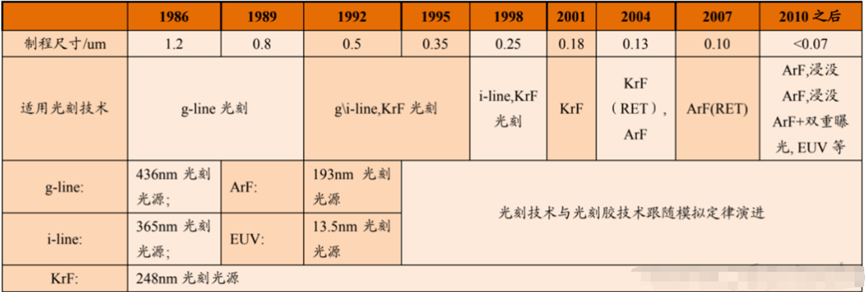
light source technology evolves into immersion lithography ; in dry lithography, which is opposite to immersion lithography, there is air between the lithography lens and the photoresist. The photoresist directly absorbs the ultraviolet radiation emitted by the light source and undergoes a photochemical reaction. In immersion lithography, there is a specific liquid between the lithography lens and the photoresist. These liquids can be pure water or other compound liquids. When the radiation emitted by the lithography light source passes through these liquids, it is refracted and the wavelength becomes shorter. In this way, under the premise of not changing the light source, the shorter wavelength ultraviolet light is projected onto the photoresist, which improves the resolution of the photolithography process. The left figure below shows a typical immersion lithography system. A typical immersion lithography system 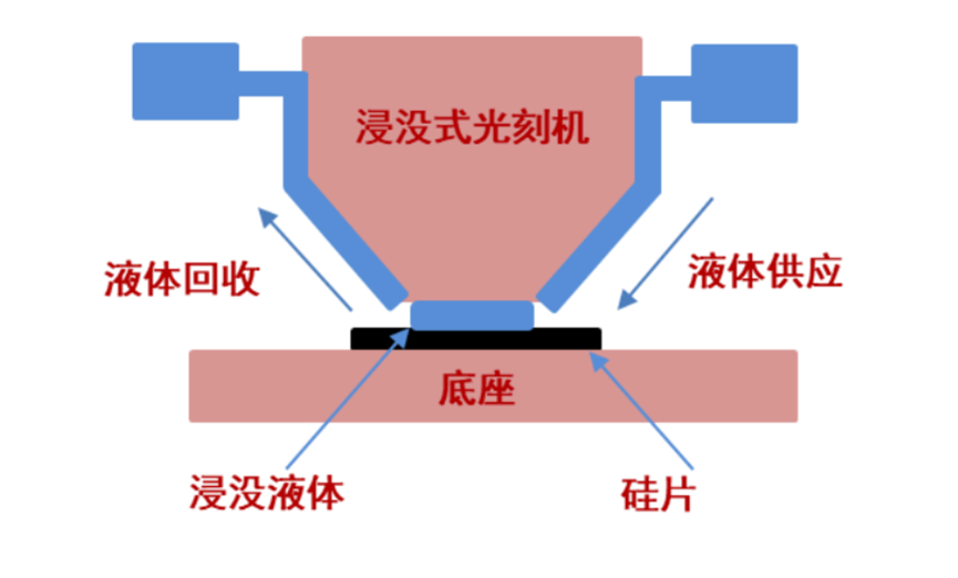
doubles the lithography ; double lithography means doubling the processing resolution by two lithography. One way to achieve this goal is to translate the same mask for the second lithography after the first lithography to improve the processing resolution. The right figure below shows such a process. The double lithography in the middle right of the figure below performs two coatings, two lithography and two etchings. With the advancement of photoresist technology, a double lithography process that only requires one coating, two lithography and one etching has become possible. 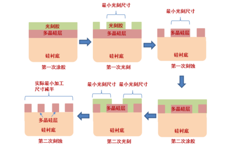
Double lithography doubles the processing resolution Immersion lithography and double lithography technologies push the processing resolution to the order of 10nm without changing the 193nm wavelength ArF lithography light source. At the same time, these two technologies also put forward new requirements for photoresists. In the immersion process, the photoresist must not react chemically with the immersion liquid or leach out and diffuse, which would damage the photoresist itself and the photolithography lens. Secondly, the refractive index of the photoresist must be greater than that of the lens, liquid and top coating. Therefore, the refractive index of the main resin in the photoresist is generally required to be above 1.9. Next, the photoresist must not deform during the immersion in the immersion liquid and the subsequent baking process, which would affect the processing accuracy. Finally, when the target resolution of the immersion process is close to 10nm, the trade-offs of multiple performance indicators of the photoresist will be more stringent. The difficulty of preparing immersion ArF photoresist is greater than that of dry ArF photoresist, which is one of the keys to the ArF photolithography processing resolution exceeding 45nm. 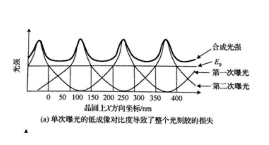
Unqualified double exposure In the double exposure process, if the photoresist can accept multiple photolithography exposures without photochemical reactions in the area blocked by the mask, one etching, one coating and one photoresist cleaning process can be saved. The left figure below shows an unqualified double exposure process. Since the photoresist in the non-exposed area still receives a relatively small amount of lithography radiation, after the two exposure processes, the radiation received by the non-exposed area may exceed the exposure threshold E0 of the photoresist, resulting in an erroneous lithography reaction. In the right middle of the figure below, the radiation energy received by the photoresist in the non-exposed area after two exposures is still less than its exposure threshold E0, so the right side of the figure below is a qualified double exposure. From this example, it can be seen that, unlike single exposure, double exposure requires a trade-off between the exposure threshold of the photoresist and the illumination intensity of the lithography light source. 
Qualified double exposure EUV (extreme ultraviolet) lithography technology is the latest development in the field of lithography in 20 years. Since the currently available optical materials cannot well support the reflection and transmission of radiation with a wavelength below 13nm, EUV lithography technology uses ultraviolet light with a wavelength of 13.5nm as the lithography light source. EUV (extreme ultraviolet) lithography technology continues to advance semiconductor process technology in the area below 10nm. At the 13.5nm wavelength scale of EUV lithography, the quantum uncertainty effect begins to emerge, bringing unprecedented challenges to the design and use of corresponding light sources, masks and photoresists. At present, only ASML in the Netherlands has the ability to manufacture EUV lithography machines, and many corresponding technical details are still unknown to the outside world. In the upcoming EUV lithography era, the industry expects that the KrF and ArF photoresist technologies that have been popular for 20 years may usher in a comprehensive technological change. Photoresist material preparation barriers are high . The microelectronic chemicals to which photoresists belong are the intersection of the electronics industry and the chemical industry, and are typical technology-intensive industries. Engaging in the microelectronic chemicals business requires key production technologies that match the cutting-edge development of the electronics industry, such as mixing technology, separation technology, purification technology, and analytical inspection technology, environmental treatment and monitoring technology that match the production process. At the same time, the diverse use scenarios of the downstream electronics industry require microelectronic chemical manufacturers to have strong supporting capabilities, and to develop and improve product processes in a timely manner to meet the personalized needs of customers. The main process of the photoresist production process is to mix the main raw materials such as photosensitive materials, resins, solvents, etc. in a constant temperature and humidity 1000-level yellow light clean room, fully stir them under the protection of nitrogen gas, make them fully mixed to form a homogeneous liquid, and filter them multiple times, and pass the intermediate process control and inspection to make them meet the process technology and quality requirements . Finally, the product is inspected and packaged, marked, and stored under the protection of nitrogen gas after passing the inspection. The entire process can be shown in the following figure: 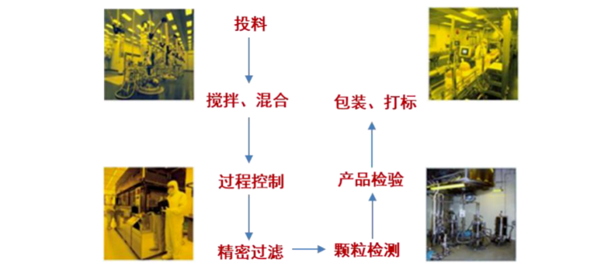
Brief flow of the production process of photoresist The technical barriers of photoresist include formulation technology, quality control technology and raw material technology. Formulation technology is the core of photoresist to realize its function, quality control technology can ensure the stability of photoresist performance, and high-quality raw materials are the basis of photoresist performance. Formulation technology: Since the downstream users of photoresist are IC chip and FPD panel manufacturers, different customers will have different application requirements, and the same customer will also have different photolithography application requirements. Generally, a semiconductor chip needs to undergo 10-50 photolithography processes during the manufacturing process. Due to different substrates, different resolution requirements, different etching methods, etc., different photolithography processes have different specific requirements for photoresists. Even for similar photolithography processes, different manufacturers will have different requirements. In response to the above different application requirements, there are many varieties of photoresists, and these differences are mainly achieved by adjusting the formulation of photoresists. Therefore, adjusting the formulation of photoresists to meet differentiated application requirements is the core technology of photoresist manufacturers. Quality control technology: Since users have high requirements for the stability and consistency of photoresists, including consistency between different batches, they usually hope to maintain a high level of consistency in photosensitivity and film thickness. Therefore, photoresist manufacturers must not only be equipped with complete testing instruments, but also establish a strict QA system to ensure the stability of product quality. Raw material technology: Photoresist is a complex and precise formula product that has been strictly designed. It is made of raw materials of different properties such as film formers, photosensitizers, solvents and additives, through different arrangements and combinations, and through complex and precise processing technology. Therefore, the quality of photoresist raw materials plays a key role in the quality of photoresists. For the purity of semiconductor chemical reagents, the International Semiconductor Equipment and Materials Organization (SEMI) has formulated international unified standards, as shown in the following table. 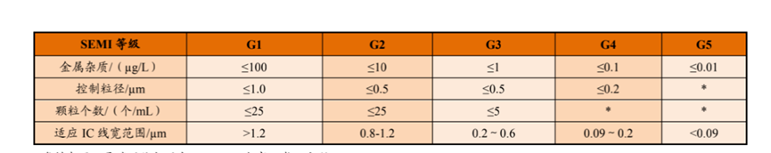
SEMI ultra-clean high-purity reagent standards The purity requirements for reagent materials used in semiconductor integrated circuits are relatively high, basically concentrated at the SEMI G3 and G4 levels. There is still a large gap between my country's research and development level and the international level; the purity requirements for ultra-clean high-purity reagents for semiconductor discrete devices are lower than those for integrated circuits, basically concentrated at the SEMI G2 level, and the production technology of domestic enterprises can meet most production needs; the level requirements for ultra-clean high-purity reagents in the flat panel display and LED fields are SEMI G2 and G3 levels, and the production technology of domestic enterprises can meet most production needs. Microelectronic chemicals, including photoresists, have the characteristics of high technical requirements, strong functionality, and fast product updates. Their product quality has a very large impact on the quality and efficiency of downstream electronic products. Therefore, downstream companies attach great importance to the quality and supply capacity of microelectronic chemical suppliers, and often adopt a certified procurement model, which requires strict screening processes such as sample inspection, technical discussion, information feedback, technical improvement, small batch trial production, large-scale supply, and after-sales service evaluation. The certification time is long and the requirements are strict; it takes a long time for general products to be certified by downstream customers. The display panel industry is usually 1-2 years, and the certification cycle of the integrated circuit industry can reach 2-3 years due to its high requirements; during the certification stage, the photoresist supplier has no income from the customer, which requires the supplier to have sufficient financial strength. Photoresist suppliers have a high stickiness with customers; generally, in order to maintain the stability of photoresist supply and effect, downstream customers will not easily change photoresist suppliers once they establish a supply relationship. By establishing a feedback mechanism to meet personalized needs, the stickiness between photoresist suppliers and customers continues to increase. Latecomers who want to join the ranks of suppliers often need to meet higher requirements than existing suppliers. Therefore, the photoresist industry has high barriers to new entrants. Usually, microelectronic chemicals such as photoresists not only have high quality requirements, but also require a variety of different categories to meet the diverse needs of downstream customers. Without economies of scale, suppliers cannot afford the expenses brought by meeting high-quality and diverse needs. Therefore, the scale of varieties constitutes an important barrier to entering the industry. At the same time, general microelectronic chemicals are corrosive to a certain extent, have high requirements for production equipment, and the production environment needs to be dust-free or dust-free. The preparation of high-end microelectronic chemicals also requires a fully enclosed and automated process to avoid pollution and improve quality. Therefore, the production of microelectronic chemicals such as photoresist has high requirements in terms of safe production, environmental protection equipment, production process system, process control system and R&D investment. Without strong financial strength, it is difficult for enterprises to gain competitive advantages in equipment, R&D and technical services to enhance sustainable development capabilities. Therefore, microelectronic chemical industries such as photoresist have high capital barriers. The photoresist industry, which is dominated by the United States and Japan, has extremely high industry barriers, so its industry is oligopolistic worldwide. The photoresist industry has been monopolized by professional companies in Japan and the United States for many years. At present, the top five manufacturers account for 87% of the global photoresist market, and the industry concentration is high. Among them, the combined market share of Japan's JSR, Tokyo Ohka, Shin-Etsu and Fuji Electronic Materials reaches 72%. In addition, the core technologies of high-resolution KrF and ArF semiconductor photoresists are basically monopolized by Japanese and American companies, and most of the products come from Japanese and American companies, such as DuPont, JSR Co., Ltd., Shin-Etsu Chemical, Tokyo Ohka Industry, Fujifilm, and Dongjin of South Korea. From the perspective of the entire photoresist market, Japan is the gathering place of giants in the photoresist industry. 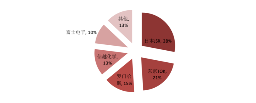
Market share of global photoresist manufacturers Japan-South Korea material friction: the localization of semiconductor materials is an inevitable trend; in July 2019 , against the background of the Japan-South Korea trade dispute, Japan announced an embargo on three semiconductor industry materials to South Korea, including etching gas, photoresist and fluoropolyimide. South Korea is a global memory production base, display production base, and global wafer foundry base. Samsung, Hynix, Eastern High-Tech and a large number of wafer foundries and display factories need Japanese semiconductor materials. These three materials directly cut off the economic pillars of South Korea's memory and display. After the embargo, South Korea's semiconductor industry faced an unprecedented crisis. For a time, global memory leaders such as Samsung Semiconductor and Hynix were in a constant shutdown crisis, and Samsung's own material inventory could only support 3 months of production. Samsung and Hynix executives also frequently went to Japan for negotiations. This is the case between Japan and South Korea, both important allies of the United States, and the Chinese technology industry, which is still in the early stages of development, needs to sound the alarm. At present, mainland China relies heavily on foreign countries for electronic materials, especially photoresists. Therefore, domestic substitution in semiconductor materials is an inevitable trend. Sino-US trade friction: Domestic substitution of photoresist is an urgent need for China's semiconductor industry; since the Sino-US trade friction, mainland China has actively laid out the integrated circuit industry. In the field of semiconductor materials, photoresist, as the "fuel" for the advancement of integrated circuit process technology, is an important link in domestic substitution and a product that will be localized. Photolithography is the core process of semiconductor process and plays a decisive role in manufacturing more advanced integrated circuits with higher transistor density. Each new generation of photolithography process requires a new generation of photoresist technology to match. Now, a semiconductor chip generally requires 10-50 photolithography processes during the manufacturing process. Different photolithography processes also have different specific requirements for photoresist. If the performance of photoresist does not meet the standards, it will have a significant impact on the chip yield. At present, the level of localization of photoresist in China is seriously insufficient, and the key technology gap is in the field of semiconductor photoresist, with a gap of 2-3 generations. With the rapid development of downstream semiconductor industry, LED and flat panel display industry, there is huge room for domestic substitution of domestic photoresist products in the future. Today, China leverages the resources of the whole society to invest in and support the semiconductor industry through the National Integrated Circuit Industry Investment Fund (Big Fund). At the same time, domestic photoresist companies are actively seizing the century-old opportunity of China's wafer manufacturing expansion to develop photoresist businesses, striving to catch up with the international advanced level as soon as possible and enter the supply chain of newly built domestic wafer fabs. The localization of photoresist is in full swing, and in the field of panel display photoresist, a number of competitive local companies have emerged in China. In the field of semiconductor and panel photoresist, although domestic photoresist still lags behind the international advanced level, with the support of policies and their own unremitting efforts, a number of photoresist companies in China have achieved technological breakthroughs. 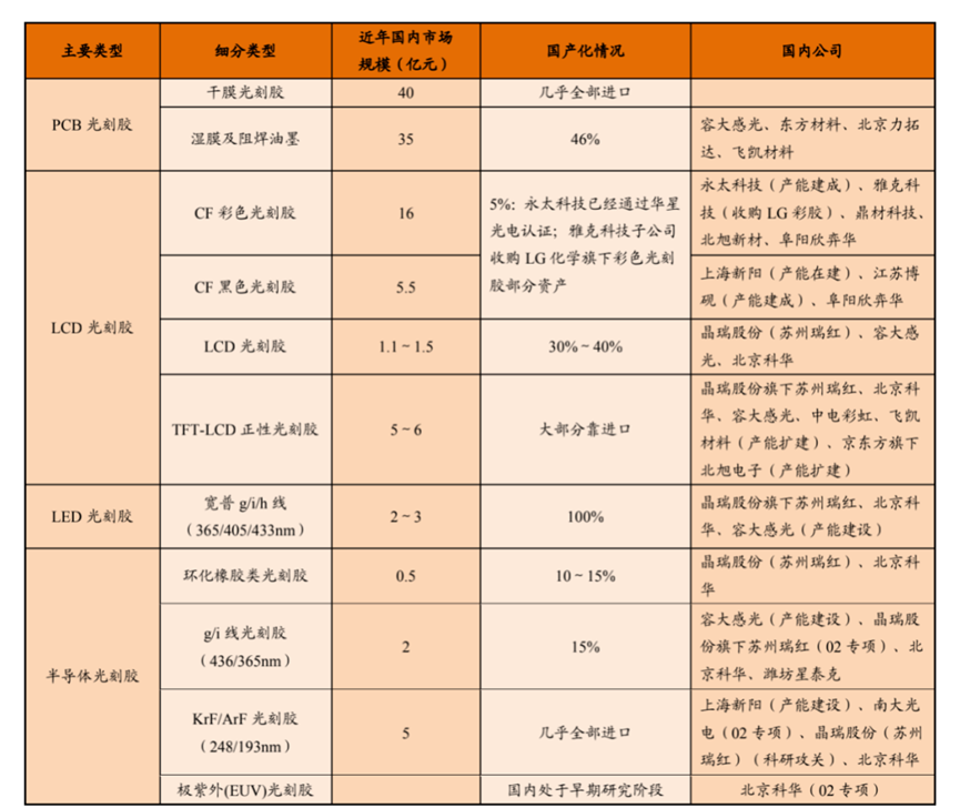
Major domestic photoresist manufacturers and domestic substitution

